Laboratories and equipment on Experimental Physics
At the Experimental Physics subject we have several advanced instruments for synthesis and characterization of nanomaterials and devices such as solar cells.
Quantum efficiency equipment
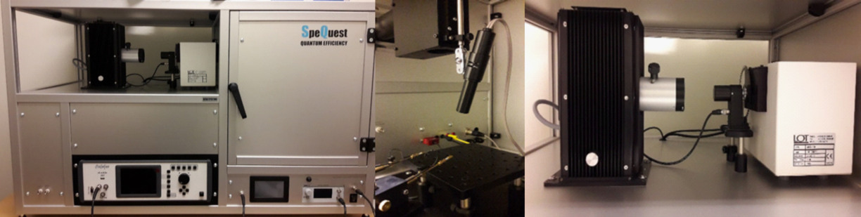
ReRa Quantum efficiency measurement station
Sample preparation/synthesis equipment
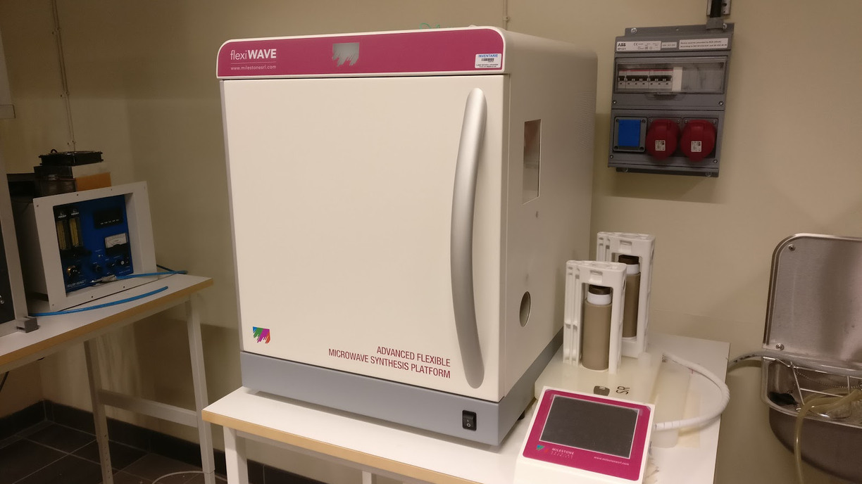
Milestone flexiWAVE
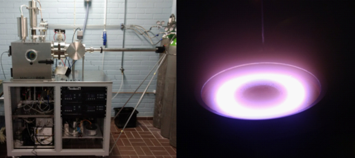
Moorfield MINILAB 060 magnetron sputter coating system
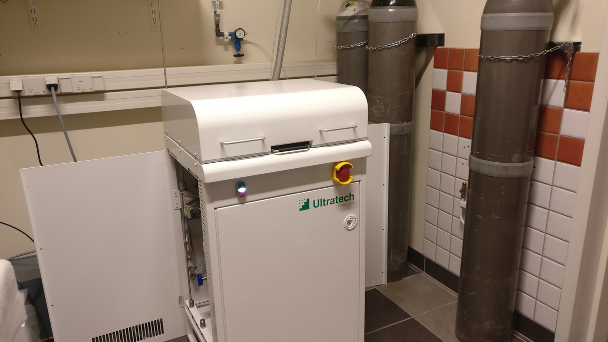
Atomic Layer Deposition (ALD), Savannah 200 Instrument
Thin film technology is used in wide range areas like electronic and optoelectronic devices, energy harvesting (photovoltaic devices), energy storage (batteries) and coating material for drug delivery applications. A fundamental step in thin film deposition is controlled synthesis of material during the deposition process to achieve a uniform thin film. Atomic Layer Deposition (ALD) is a technique that allows the growth of thin films, in atomic scale from a few tens of nanometer (a single layer of atoms or molecules) up to micrometer (several layer of atoms or molecules), layer by layer. The ALD system at Experimental Physics in LTU, Savannah 200 from Ultratech/Cambridge Nanotech, operates in continuous mode and exposure mode. The continuous mode enables to deposit a thin film that is uniform, conformal and perfectly dense rapidly. In the exposure mode, we are able to coat high aspect ratio materials like porous materials, fibers and nanogels. There is possibility to grow different types of films like oxides (Al2O3, Co3O4, TiO2, SiO2, ZnO, ZrO2, In2O3, SnO2, Ga2O3, MoO3, V2O3), doped oxides (AZO, ATO, ITO), Nitrides (Zr3N4, AlN, TiN), and sulfide (ZnS).
Electrochemical characterization equipment
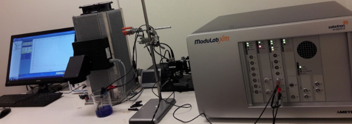
ModuLab XM ECS Electrochemical Test System
Optical spectroscopy equipment
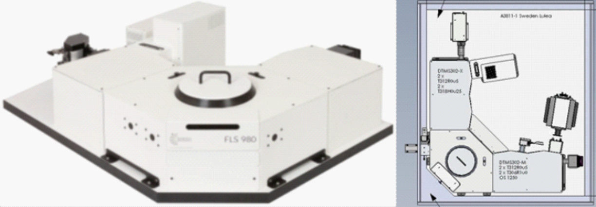
Edinburgh Instruments FLS980 spectrofluorimeter
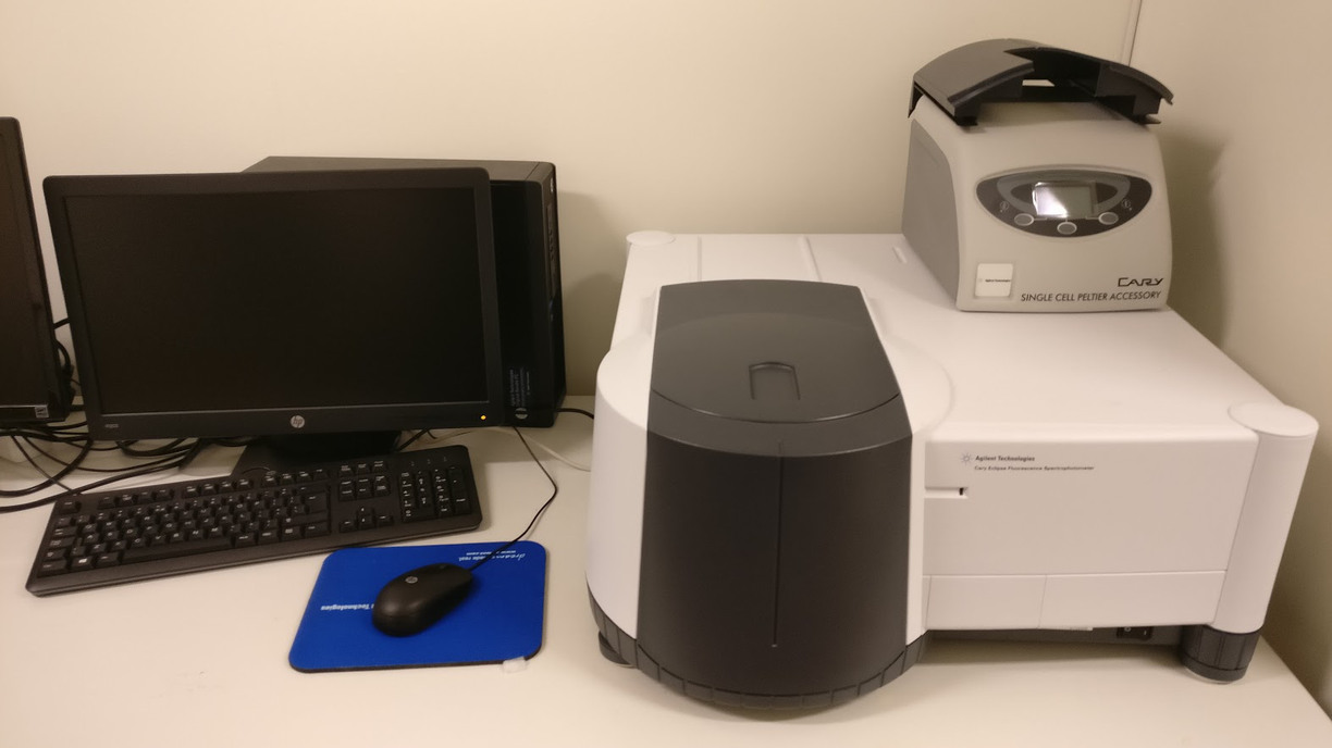
Agilent Cary Eclipse fluorescence spectrometer
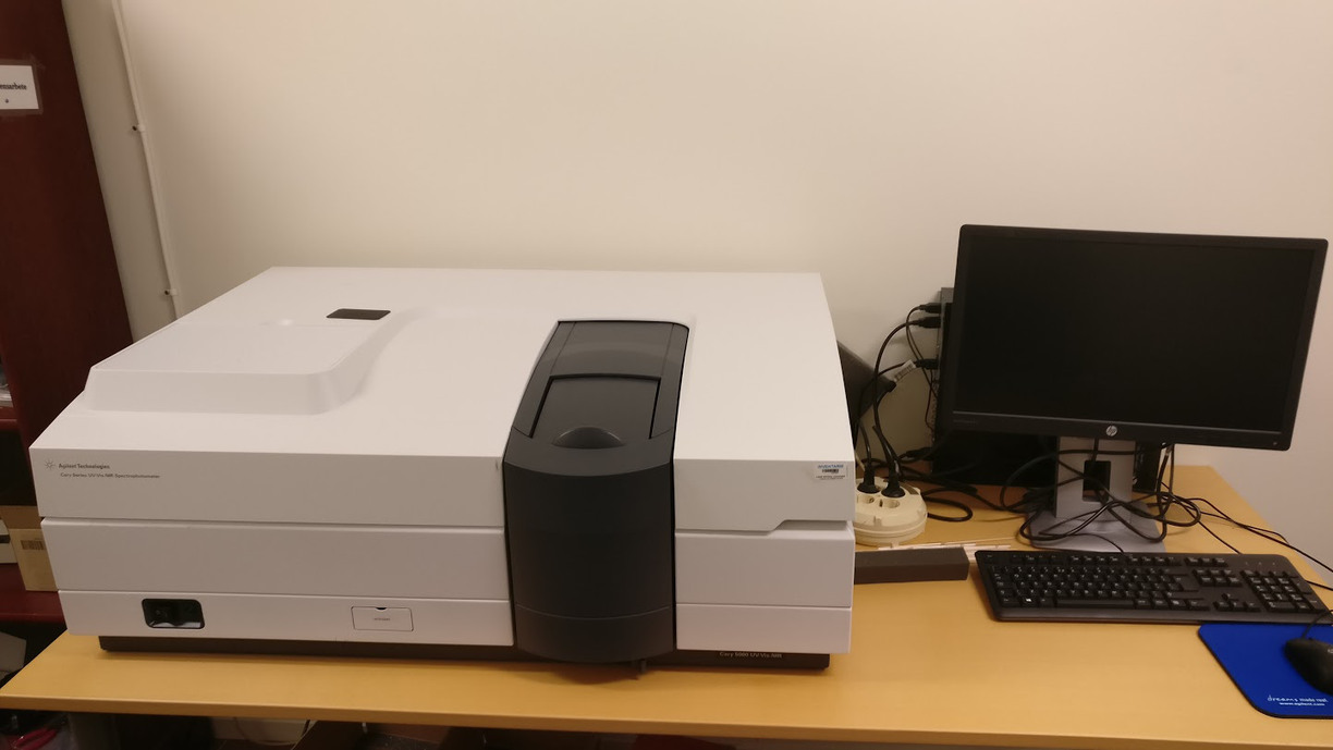
Agilent Cary 5000 spectrophotometer
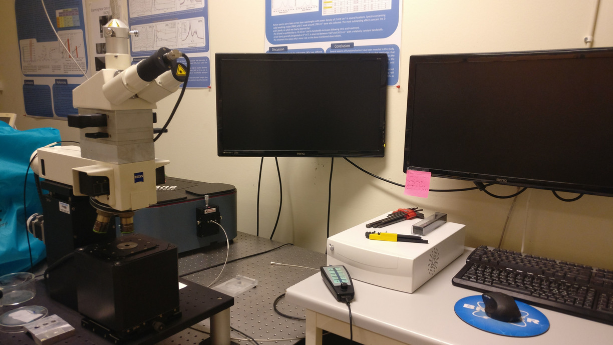
WiTec CRM-200 Raman/fluorescence microscope/imaging system
The CRM-200 system includes a single stage spectrometer with an IR-enhanced CCD and an APD, a system of notch filters and photonic crystal-based fiber optics.
Available excitation lasers:
- Spectra physics Millenia V, 532 nm, 5 W max output power
- Coherent, 633 nm, 30 mW max output power
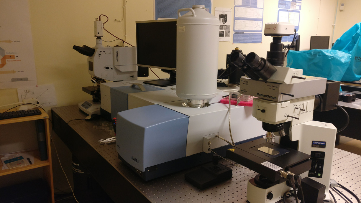
Bruker FT-Raman & FTIR
Our IR spectroscopy equipment consists of:
- Vertex 70v vacuum-based FTIR spectrometer for measurements in mid- and near-IR range.
- Hyperion 2000 IR microscope with ATR attachments and long-working distance objectives.
- FT-Raman module and microscope with 1064 nm excitation laser (1000 mW).
Equipment for high-pressure spectroscopy
We have a number of Diamond Anvil Cells (DACs) to generate high pressure (up to 0.5 MBar routinely achievable and well-controlled in these devices):
- Membrane DAC equipped with an internal heater (up to 900 °C).
- Plate DAC with type II-a diamond anvils dedicated for IR measurements.
- Membrane DAC with designed (electrical probes lithographically patterned on the
anvil surface) diamond anvil for resistance measurements at ultra-high pressures (loan
from National Lawrence Livermore Lab, Berkeley, USA). - Plane/cone DAC for fast resistance measurements at high pressure.
A setup for ultra-high resistance measurements:
- Agilent 4339B Electrometer (resistance measurements limit 10 TOhm).
- Agilent 34411, a High-speed Digital Multimeter (resolution 0.1 microVolt).
- Agilent 34980, a 48-channel digital scanning system for high-precision measurements of resistance, capacitance, temperature.
Sample preparation:
- Betsa Electric Discharge Machine (EDM) for drilling small holes (down to 50
micrometers in diameter) in metallic gaskets for loading DAC samples. - Olympus BX51 materials research microscope equipped with epi-fluorescence
attachment, differential interference contrast (DIC) setup and a set of objectives for high-resolution imaging. - Sonics ultra-high power ultrasonic disperser for tip sonication/debundling of carbon
nanotubes.
Updated:
Page author: Contact us